| Prev | Next |
Electrical Circuit Simulation Example
In this section, we will walk through the creation of a SysML parametric model for a simple electrical circuit, and then use a parametric simulation to predict and chart the behavior of that circuit.
Circuit Diagram
The electrical circuit we are going to model, shown here, uses a standard electrical circuit notation.
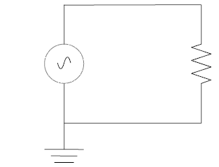
The circuit includes an AC power source, a ground and a resistor, connected to each other by wires.
Create SysML Model
This table shows how we can build up a complete SysML model to represent the circuit, starting at the lowest level types and building up the model one step at a time.
Component |
Action |
|---|---|
|
Types |
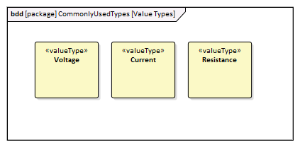
Define Value Types for the Voltage, Current and Resistance. Unit and quantity kind are not important for the purposes of simulation, but would be set if defining a complete SysML model. These types will be generalized from the primitive type 'Real'. In other models, you can choose to map a Value Type to a corresponding simulation type separate from the model.
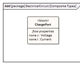
Additionally, define a composite type called ChargePort, which includes properties for both Current and Voltage. This type allows us to represent the electrical energy at the connectors between components.
|
|
Blocks |
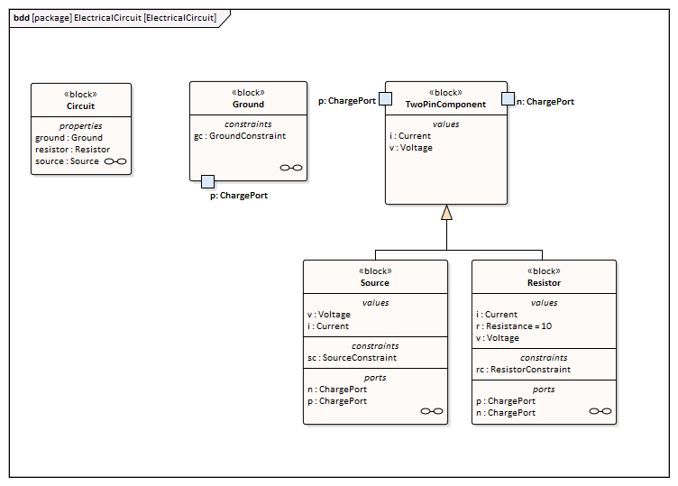
In SysML, the circuit and each of the components will be represented as Blocks. Create a Circuit Block in a Block Definition diagram (BDD). The circuit has three parts: a source, a ground, and a resistor. These parts are of different types, with different behaviors. Create a Block for each of these part types. The three parts of the Circuit Block are connected through Ports, which represent electrical pins. The source and resistor have a positive and a negative pin. The ground has only one pin, which is positive. Electricity (electric charge) is transmitted through the pins. Create an abstract block 'TwoPinComponent' with two Ports (pins). The two Ports are named 'p' (positive) and 'n' (negative), and they are of type ChargePort. This figure shows what the BDD should look like, with the blocks Circuit, Ground, TwoPinComponent, Source and Resistor.
|
|
Internal Structure |
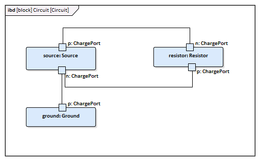
Create an Internal Block diagram (IBD) for Circuit. Add properties for the Source, Resistor and Ground, typed by the corresponding Blocks. Connect the Ports with connectors. The positive pin of the Source is connected to the negative pin of the Resistor. The positive pin of the Resistor is connected to the negative pin of the Source. The Ground is also connected to the negative pin of the Source.
Notice that this follows the same structure as the original circuit diagram, but the symbols for each component have been replaced with properties typed by the Blocks we have defined. |
|
Constraints |
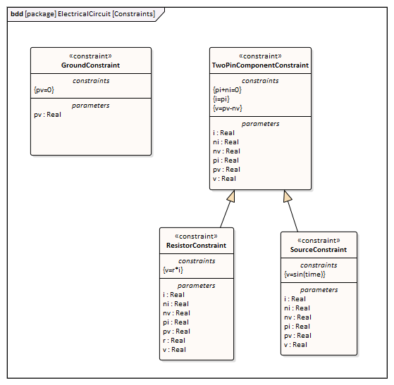
Equations define mathematical relationships between numeric properties. In SysML, equations are represented as constraints in Constraint Blocks. Parameters of Constraint Blocks correspond to SimVariables and SimConstants of Blocks ('i', 'v', 'r' in this example), as well as to SimVariables present in the type of the Ports ('pv', 'pi', 'nv', 'ni' in this example). Create a Constraint Block 'TwoPinComponentConstraint' to define parameters and equations common to sources and resistors. The equations should state that the voltage of the component is equal to the difference between the voltages at the positive and negative pins. The current of the component is equal to the current going through the positive pin. The sum of the currents going through the two pins must add up to zero (one is the negative of the other). The Ground constraint states that the voltage at the Ground pin is zero. The Source constraint defines the voltage as a sine wave with the current simulation time as a parameter. This figure shows what these constraints should look like in a BDD.
|
|
Bindings |
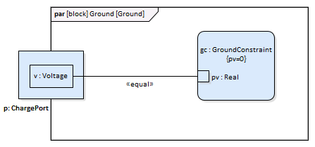
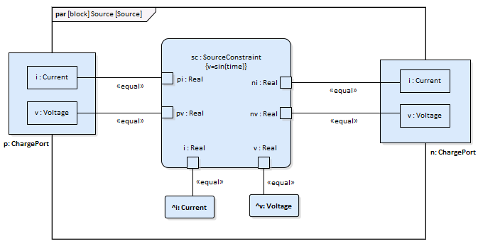
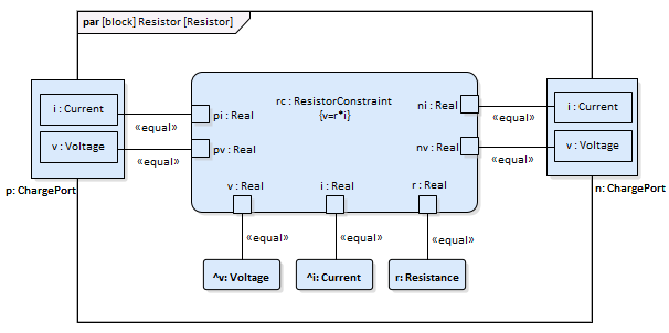
The values of Constraint parameters are equated to variable and constant values with binding connectors. Create Constraint properties on each Block (properties typed by Constraint Blocks) and bind the Block variables and constants to the Constraint parameters to apply the Constraint to the Block. These figures show the bindings for the Ground, the Source and the Resistor respectively. For the Ground constraint, bind gc.pv to p.v.
For the Source constraint, bind:
For the Resistor constraint, bind:
|
Configure Simulation Behavior
This table shows the detailed steps of the configuration of SysMLSim.
Step |
Action |
|---|---|
|
SysMLSimConfiguration Artifact |
|
|
Create Root elements in Configuration Manager |
|
|
ValueType Substitution |
Expand ValueType and for each of Current, Resistance and Voltage select 'SysMLSimReal' from the 'Value' combo box. |
|
Set property as flow |
|
|
SysMLSimModel |
This is the model we want to simulate: set the block 'Circuit' to be 'SysMLSimModel'. |
Run Simulation
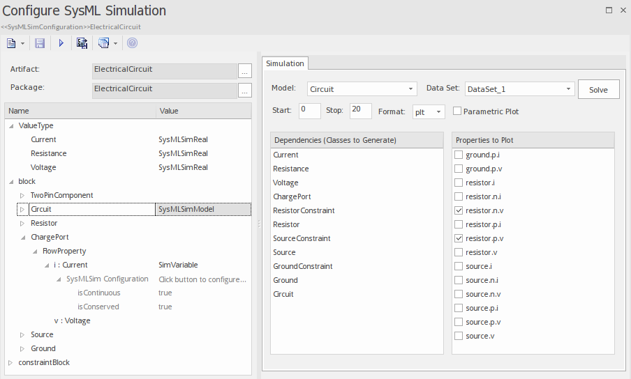
In the 'Simulation' page, select the checkboxes against 'resistor.n.v' and 'resistor.p.v' for plotting and click on the .
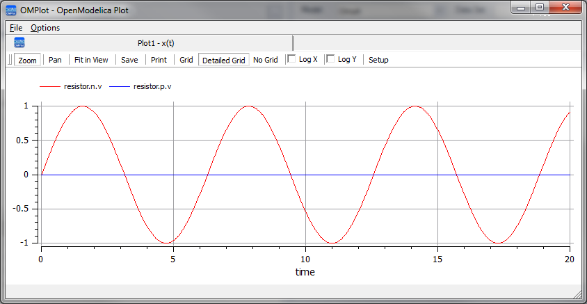
The two legends 'resistor.n.v' and 'resistor.p.v' are plotted, as shown.
 button to open the 'Element Configurations' dialog
